The Day Chips Stopped Talking About Intelligence and Started Talking About Work
- This morning, at the Santa Clara AI infrastructure summit, a number the semiconductor industry had never once uttered was read aloud. The speed at which an agent works: 1000 tokens per second. On the same stage, a verdict of a different nature was delivered. CXL, the cheap memory that could have stood in for soaring HBM, received a “death certificate” from the people who actually run models. Today’s semiconductor industry news is not about intelligence. The subject of the talk is “work.” In other words, this post reads all of today’s chip and memory news through a single lens: how fast an agent works, and what that work costs.
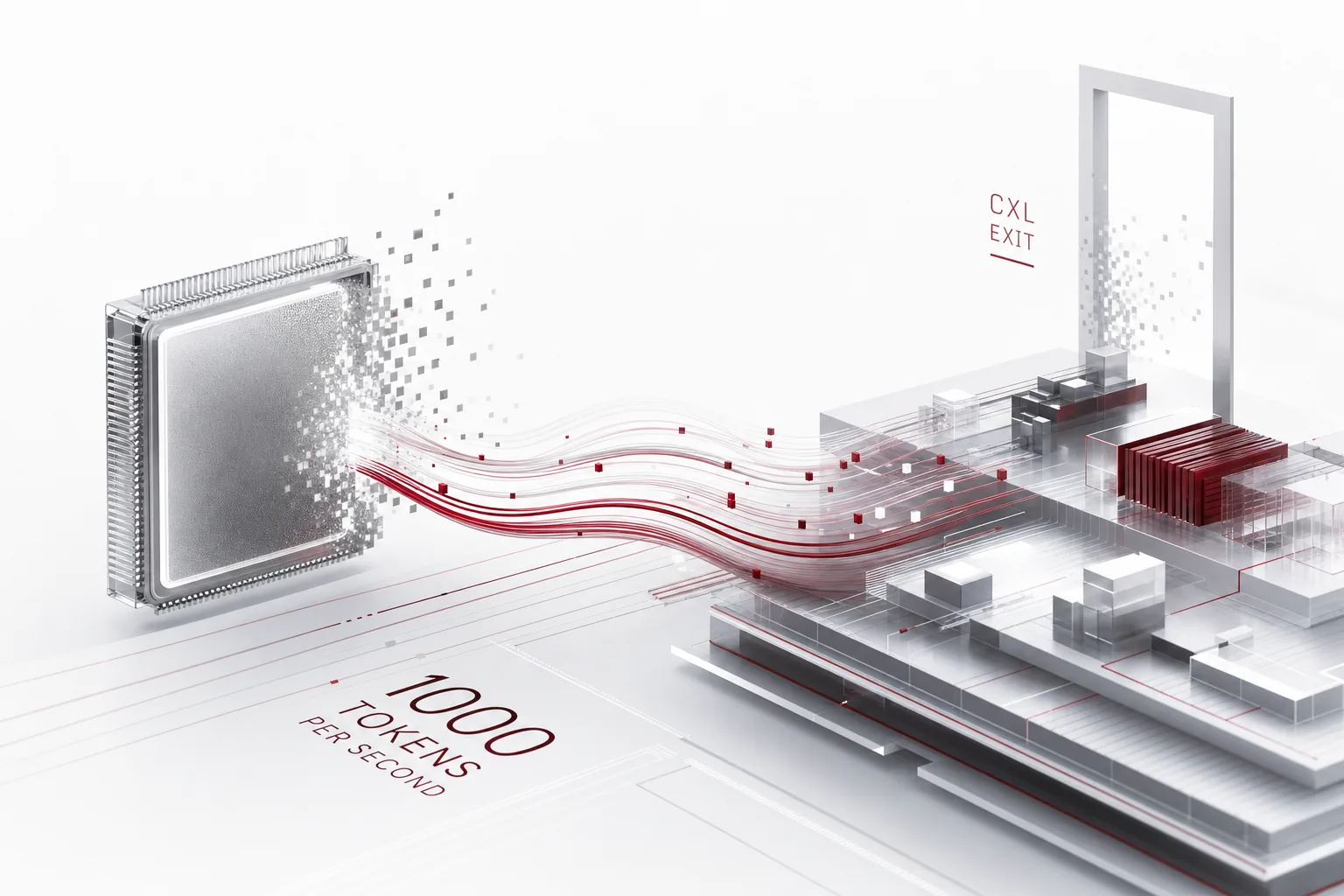 A visualization of the post’s core concept.
The Death of Cheap Memory
The story begins with the “death” that happened at the summit. Daniel Morris, a researcher in charge of AI accelerator design at OpenAI, said he could not find any CXL use cases from the standpoint of actually running models. Intel’s head of SoC architecture described CXL memory bundles as “a complement to secondary storage, not an HBM replacement,” and pointed out that GPU data speeds do not reach HBM’s.
It is not that CXL was unprepared. The CXL 4.0 spec pushed bandwidth up to 128GTs, and the CXL consortium touted memory expansion and sharing at the same summit. CXL is a fabric technology focused on capacity expansion, memory pooling, and multi-host sharing, and it has never competed with HBM, the stacked memory attached directly to the processor, on the bandwidth front. Even so, the venue where the model operators and the silicon suppliers simultaneously said “there are no use cases” was a big one. That CXL will remain a capacity auxiliary rather than a bandwidth substitute is, in effect, the industry’s confirmation. The industry’s hope of swapping HBM for CXL to lower AI server build costs has taken a step back.
The timing of this verdict is no accident. The memory supercycle in AI data centers is in full swing. Bank of America forecast the 2026 HBM market at $54.6 billion, a 58% increase year over year, and Goldman Sachs projected that HBM demand for custom ASICs will surge 82% to account for a third of the market. When memory becomes this scarce, the industry naturally looks for a cheap substitute. For a while, that substitute was CXL.
The CXL story is not fully over. In roles such as long-context inference and KV cache offloading, it remains a capacity complement. Only the narrative that “it stands in for HBM’s bandwidth” is closed for the time being.
The Chip Changed Its Unit
So the memory companies change their unit. Not FLOPS and not capacity. The number Samsung’s senior executive Kim In-dong put on the table is “1000 tokens per second.” The response speed of conversational AI is on the order of 100 tokens per second, and the goal is to raise that figure tenfold for agentic AI. The vehicle is zHBM, a 3D vertically stacked memory that claims up to 8x the performance and more than 3x the power efficiency of HBM5. A roadmap for zNAND-O, an on-device storage, was released alongside it: sample supply in 2028, running a 1-trillion-parameter model on a single workstation in 2030, and one-sixth the cost of DRAM alone.
The competition is not confined to the future. Samsung began mass-production shipments of HBM4 for NVIDIA’s next-generation accelerator Vera Rubin in February, ahead of the industry, and shipped the world’s first HBM4E 12-stack at the end of May. The analysis is that whoever sets the heat and packaging standards that 3D stacking will bring will be the key variable determining the supply structure of next-generation AI accelerators.
A shift in the competitive landscape is mixed in as well. SK Hynix’s HBM market share fell from 62% in the second quarter of 2025 to 50% in the second quarter this year. In that same stretch, Samsung closed the gap to 17 points. The contest over the memory that will determine agent speed has effectively become a head-on duel.
In the background is the so-called memory wall. GPU computation runs ahead of the growth in memory bandwidth and capacity, and the bottleneck migrates to memory. Here, an agent and a chatbot are different creatures. A chatbot answers once and is done, but an agent holds a task in mind, calls tools, verifies, and revises again. The longer the context, the larger the “working memory” required. For an agent, memory is like the working memory the human brain has, and that is exactly why Samsung calls agent memory the decisive contest.
Verification, More Than Half of a Chip’s Life
And the company itself has already let an agent into its own workplace. Samsung’s System LSI has been running a pilot since May of this year, deploying Claude Code to chip design verification work for 3 months. It automatically generates test scenarios and finds latent defects. Choi Ki-young, Anthropic’s Korea representative, who confirmed the application test, argued that “there had been no precedent for automating manual design verification with AI,” and as a counterpoint the case of OpenAI and Broadcom taping out their own inference chip in 9 months was put on the table at the same time. The specific deployment scale and contract terms have not been disclosed, and final review and approval by design engineers is required for any output the AI derives.
The direction of diffusion is also clear. Once the effective defect detection rate of test code derived by the AI is proven, it will spread through the design house ecosystem and become a standard in foundry standard design environments. Shortening chip development schedules will emerge as a differentiating factor in system semiconductor competition; conversely, if errors mix into generated outputs and rework increases, the effect is halved.
The axis of competitiveness is shifting too. The semiconductor competitiveness once measured by engineer headcount is being remeasured as “inference cost structure and verification reliability.” The trend of LLM companies digging into the core workflow of semiconductor R&D is also becoming clear. Anthropic has reportedly started designing its own AI chip and is considering using Samsung’s 2-nanometer process.
The weight of verification is no small thing. The EDA market is monopolized at more than 80% by the three Western firms Synopsys, Cadence, and Siemens EDA, and verification is a bottleneck that consumes more than half of a chip development schedule. What matters more than the pilot is the cost attached behind it. The front side of the price is surprising. Claude Fable 5.1’s cache read rate is $0.25 per 1 million tokens, a 75% reduction. Yet the weighted average cost per complex real-world task is $3.69, up 58% from the previous generation. The price of “intelligence” fell and the cost of “work” rose. An agent’s work is not a single question. It is long context, multiple steps, tool calls, and repeated retries. The unit of enterprise AI cost is moving from “how smart is the model” to “how much work gets done.” Meanwhile, China’s Empyrean is shortening circuit placement and simulation from 4 weeks to 1 week with an agentic EDA platform that integrates an AI agent, and is switching its business model from an annual license to token-based metering. The verification process tied up in an annual license is becoming a business broken down by the token.
The Supply Map Is Redrawn Too
While the unit changes, the map moves too. According to Reuters on the 16th, SK Hynix is negotiating with Intel a plan to produce memory chips in the United States for the first time. Leasing part of Intel’s Ohio facility and a joint-venture scenario with cloud-company customers participating are both on the table. Behind it sits the U.S. Commerce Secretary’s semiconductor tariff card. SK Hynix is already building an HBM advanced packaging fab in West Lafayette, Indiana for roughly $4 billion, with mass production targeted for the second half of 2029. Even amid the memory price rally, the limit of customers’ endurance is starting to show. The price increase for commodity DRAM and NAND in the third quarter is expected to slow from the 60% range in the previous quarter to the mid-to-high teens.
The flow of inference workloads is taking root locally as well. Domestic NPU startup Rebellion is partnering with Japan’s ai& to build more than 100 inference-specialized NPU racks, called Rebellacks, in Tokyo data centers, with a goal of securing 40MW of infrastructure by the end of 2027. ai& has secured more than $2 billion in infrastructure investment, reaching five sites in operation by the end of this year. The configuration is a heterogeneous mix of GPU and NPU, and the logic is the same. The more an agent’s work grows, the more important cost per watt and cost per token become, with the GPU handling flexibility and the NPU handling economy.
The domestic power race is heating up too. KT announced a plan to invest a total of 6 trillion won in AI infrastructure over 5 years through 2031, of which roughly 5 trillion won goes to AIDC and 1 trillion won to submarine cables, and to supply more than 1GW of AIDC across about 20 sites nationwide by 2031. The government already rolled out a policy in July to draw in 550 trillion won in private investment toward building ultra-massive AIDC of 8.4GW by 2029. In a competition where “power and land” determine the order of AI infrastructure supply, the question of where to run an agent’s work and at what cost is thrown more sharply.
Korea’s position on this map is not small. By Counterpoint’s tally, Samsung’s HBM market share rose from 21% in the previous quarter to 33% in the second quarter this year. SK Hynix is holding 50%. SK Hynix’s 2026 outlook is also focused on an “HBM-led memory supercycle.” Thanks to CXL’s defeat, the two companies’ dominance is expected to continue for a while.
What Is Missing From This Picture
Every number from this morning is telling a single story: that working speed itself has become the product. But there is one question missing from this picture. When working speed has become the product, who is the subject that checks whether the work is trustworthy?
Samsung’s pilot carried one clause as well: that final review and approval of AI output by design engineers is mandatory. Verification is work where, if it goes wrong, the fab burns. None of what a company entrusts to an agent is any different. If speed is 1000, governance must be at the same speed. Otherwise, the faster it gets, the more expensive the accident becomes. And when an accident happens, the question is who proves whose responsibility it is. Audit logs and permission isolation are no longer a nice-to-have; they become an entry condition for putting an agent onto the front line.
What aims to fill that gap is Paxis, ThakiCloud’s official product, an agent-native cloud. Paxis treats skills, tools, policies, and audit logs as first-class resources. Work is completed inside an isolated sandbox, passes a policy gate, and is recorded in an audit log. Because the model can be chosen differently per task (CostRouter), the “cost per unit of work” structure revealed by today’s news can be caught at design time rather than managed after the fact. Deployment to sovereign, on-premises K8s environments is also possible. In other words, the moment an agent’s work becomes a product that is metered and billed, a company’s question is no longer which model is good. It becomes whether the work can be run safely, and whether its trace can be verified later. If the physical layer has started selling “working speed,” what the enterprise side should ask for is a “platform of trustworthy work.”
References
This post was written by synthesizing the news below.
- Global Economic, Samsung Puts Claude Into Chip Design Verification: The Solution Found After a 3-Month Trial
- Financial News, Samsung: “zHBM Delivers 1000 Tokens per Second: The AI Agent Memory Contest”
- Korea Economy, HBM’s Lead in the AI Market Looks Set to Continue: “Cannot Be Replaced by CXL”
- SBS Biz, [Biz Now] SK Hynix and Intel Join Hands: “U.S. Production Talks”
- Aju Economy, [Economy Daily] KT, 6 Trillion Won Over 5 Years in AI Infrastructure: The Math Behind 1GW AIDC Expansion
- Edaily, Rebellion Sets Up 100+ “Rebellacks” in Tokyo, Japan: Aiming at 40MW of AI Infrastructure